ECW 2018 CTF Qualification: Escape Game
Challenge details
| Event | Challenge | Category | Points | Solves |
|---|---|---|---|---|
| ECW 2018 CTF Qualification | Escape Game | Reverse Engineering | 100 | 18 |
Description
On your way to join the ECW HeadQuarter room a door blocks you off the road.
Next to it four buttons that seem to be used to open it.
One of your friends accompanying you already seems to know the place and provides you some documents on the device.
It would be based on an electronic card based on Atmel Mega 2560.
Can you open the door?
The flag to validate will be of type 1-3-2-1-2 (the figures representing the number of consecutive buttons to press to open the door)
Link to the circuit diagram: [here]
Link to the embedded code in the microcontroller: [here]
For pin not noted on the diagram:
- button 1 : pin 22 (on the board) ; pin 78 (sur le µc) : PA0 (AD0)

- button 2 : pin 23 (on the board) ; pin 77 : PA1 (AD1)

- button 3 : pin 24 (on the board) ; pin 76 : PA2 (AD2)

- button 4 : pin 25 (on the board) ; pin 75 : PA3 (AD3)

- door : pin 5 (on the board) ; pin 5 : (OC3A/AIN1) PE3
Introduction
During the ECWCTF qualification, I worked on an interesting challenge: reversing an Arduino ROM, I’ll try to do my best to describe my methodology in this writeup.
Special mention to Thanat0s for his post that helped me solve this challenge!
Methology
Creating an Atmel 2560 configuration for IDA
The first step I did was to create an IDA configuration for Atmel 2560 because it was not implemented by default in IDA and I couldn’t find one on the Internet.
So here we go, let’s pull out our keyboard and follow the datasheet
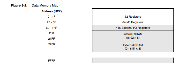
Creating a configuration for IDA is not that complex. First, we need to fill in the memory sections addresses based on the figure 8-2 from the datasheet:
Here is the result:
RAM=8192
ROM=262144
EEPROM=4096

; MEMORY MAP
;See figure 8-2
area DATA GPWR_ 	0x0000:0x001F General registers ( 32 registers )
area DATA FSR_  	0x0020:0x005F 64 I/O registers
area DATA EXTIO_	0x0060:0x01FF 416 External U/O registers
area DATA I_SRAM_	0x0200:0x21FF Internal SRAM ( 8192 * 8 )
area DATA E_SRAM_	0x2200:0xFFFF External SRAM ( 0-64K * 8 )
Then, here is the funny part (I spent a lot of time on it), we just need to implement the Register summary table in the
configuration file (4 pages):
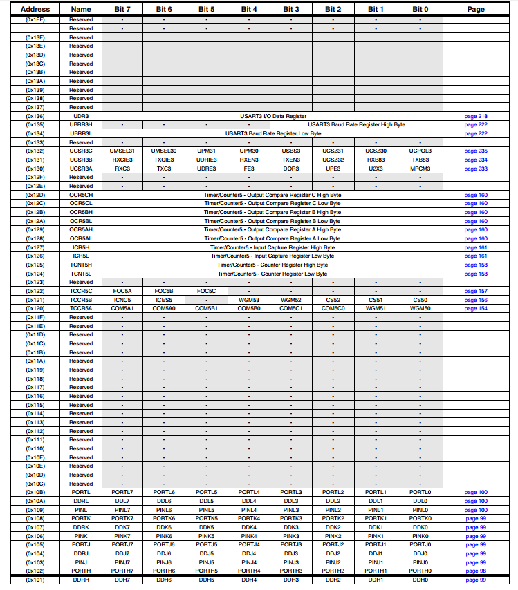
This is not really complex, we just need to scroll down and copy up the values.
So we get a file of ~400 lines that we can merge with the config/avr.cfg file in the IDA installation directory:
Finally, we can use our configuration in IDA \o/
Extracting RAM from the ROM
Now that our ROM is loaded into IDA, we are going to extract the RAM from the ROM in order to resolve variables values (useful to associate the pins to their operation).
We will therefore look for the __RESET method that will be useful to find the offsets.
We get this function:
ROM:0114 __RESET:                                ; CODE XREF: ADC__0↑j
ROM:0114                 clr     r1
ROM:0115                 out     SREG, r1
ROM:0116                 ser     r28
ROM:0117                 ldi     r29, 0x21 ; '!'
ROM:0118                 out     SPH, r29
ROM:0119                 out     SPL, r28
ROM:011A                 ldi     r16, 0
ROM:011B                 out     EIND, r16
ROM:011C                 ldi     r17, 2
ROM:011D                 ldi     r26, 0
ROM:011E                 ldi     r27, 2          ; 0x200 -> RAM address
ROM:011F                 ldi     r30, 0xB8
ROM:0120                 ldi     r31, 0x11       ; 0x11B8 -> ROM address
ROM:0121                 ldi     r16, 0
ROM:0122                 out     RAMPZ, r16
ROM:0123                 rjmp    loop_end
ROM:0124 ; ---------------------------------------------------------------------------
ROM:0124
ROM:0124 loop_copy:                              ; CODE XREF: __RESET+14↓j
ROM:0124                 elpm    r0, Z+
ROM:0125                 st      X+, r0
ROM:0126
ROM:0126 loop_end:                               ; CODE XREF: __RESET+F↑j
ROM:0126                 cpi     r26, 0x94
ROM:0127                 cpc     r27, r17
ROM:0128                 brne    loop_copy
ROM:0129                 ldi     r18, 5
ROM:012A                 ldi     r26, 0x94       ; 0x94 -> Area size to be extracted
ROM:012B                 ldi     r27, 2
ROM:012C                 rjmp    loc_12E
ROM:012D ; -----------------------------------------
So we create a RAM file containing:

This results in the following file: RAM.bin
Now, we just need to load this file into IDA segments!
Delete existing RAM segment:
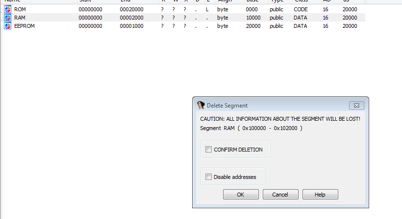
Load the RAM.bin file as RAM segment with correct alignment:
Final segments:

Here are the values associated with the right offsets:
Final part (reverse)
Let’s start reverse engineering \o/
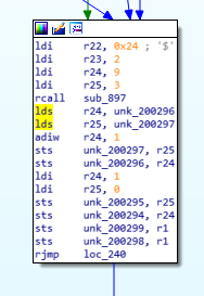
First, we will look for the setup() function that initializes the variables, this one is located at the offset 0x143:
ROM:0143 ldi r20, 0x80
ROM:0144 ldi r21, 0x25 ; '%'
ROM:0145 ldi r22, 0
ROM:0146 ldi r23, 0
ROM:0147 ldi r24, 9
ROM:0148 ldi r25, 3
ROM:0149 rcall sub_6E9
ROM:014A ldi r22, 2
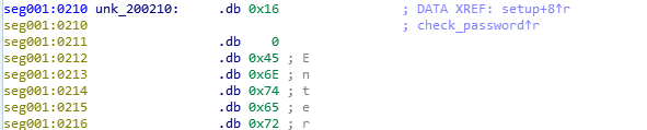
ROM:014B lds r24, unk_200210
ROM:014D rcall pin_mode
ROM:014E ldi r22, 2
ROM:014F lds r24, pin_23
ROM:0151 rcall pin_mode
ROM:0152 ldi r22, 2
ROM:0153 lds r24, pin_24
ROM:0155 rcall pin_mode
ROM:0156 ldi r22, 2
ROM:0157 lds r24, pin_25
ROM:0159 rcall pin_mode
ROM:015A ldi r22, 1
ROM:015B lds r24, pin_door
ROM:015D rcall pin_mode
ROM:015E ldi r22, 0x12
ROM:015F ldi r23, 2
ROM:0160 ldi r24, 9
ROM:0161 ldi r25, 3
ROM:0162 rjmp sub_897
Which can be translated into the following Arduino code:
int button1 = 22;
int button2 = 23;
int button3 = 24;
int button4 = 25;
int pin_door = 5;

void setup() {
	pinMode(button1, INPUT_PULLUP);
	pinMode(button2, INPUT_PULLUP);
	pinMode(button3, INPUT_PULLUP);
	pinMode(button4, INPUT_PULLUP);
	pinMode(pin_door, INPUT);
}
Now that we know how the values are initialized, we are looking for the function that will check the pin code.
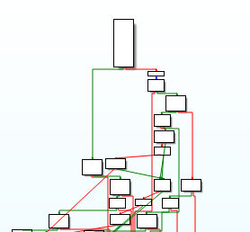
This function (a bit complex) is located at the 0x0163 offset, here is an overview:
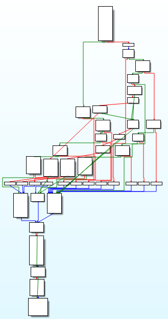
Here, I will simplify the explanation, as we can ignore a significant part that checks the pressed button:
Here comes the interesting part!
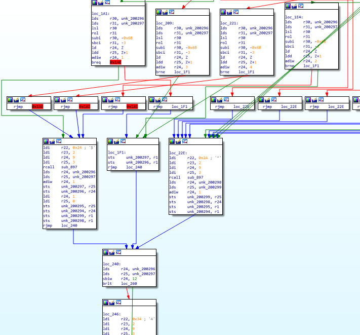
Here we have 4 blocks that will perform operations according to the pressed buttons:
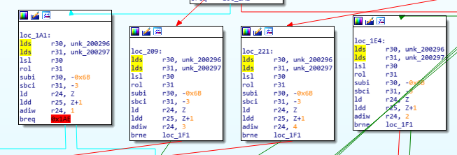
Here we have the steps that will reset or increment a counter depending on the button pressed.
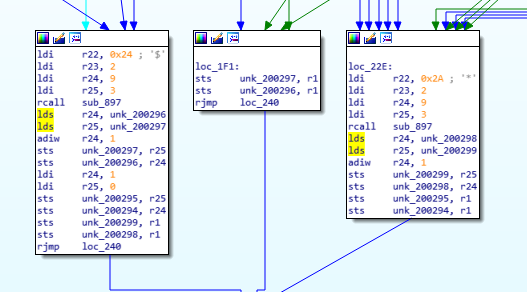
And finally a block that checks if our counter equals to 12 and in this case displays the success message.
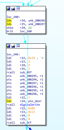
So here we will look for a way to increase our counter to 12 by using this block which increments the counter and resets the other variables of the function.
Our 4 top blocks each check a condition as follows:
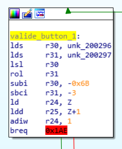
This gives us an approximative algorithm:
if (button_value + pass_table[count*2] == 0):
	goto success
else:
	goto fail
So, let’s find this pass_table in our RAM file! It’s easily found at 0x026B:
seg001:026B                 .db 0xFF
seg001:026C                 .db 0xFF
seg001:026D                 .db 0xFF
seg001:026E                 .db 0xFF
seg001:026F                 .db 0xFF
seg001:0270                 .db 0xFF
seg001:0271                 .db 0xFD
seg001:0272                 .db 0xFF
seg001:0273                 .db 0xFC
seg001:0274                 .db 0xFF
seg001:0275                 .db 0xFE
seg001:0276                 .db 0xFF
seg001:0277                 .db 0xFF
seg001:0278                 .db 0xFF
seg001:0279                 .db 0xFD
seg001:027A                 .db 0xFF
seg001:027B                 .db 0xFC
seg001:027C                 .db 0xFF
seg001:027D                 .db 0xFD
seg001:027E                 .db 0xFF
seg001:027F                 .db 0xFD
seg001:0280                 .db 0xFF
seg001:0281                 .db 0xFD
seg001:0282                 .db 0xFF
All we have to do now is take the values 1 out of 2 and we get the final flag:
1-1-1-3-4-2-1-3-4-3-3-3
Areizen